

The Dutch Miracle Machines
Creating intelligence out of sand

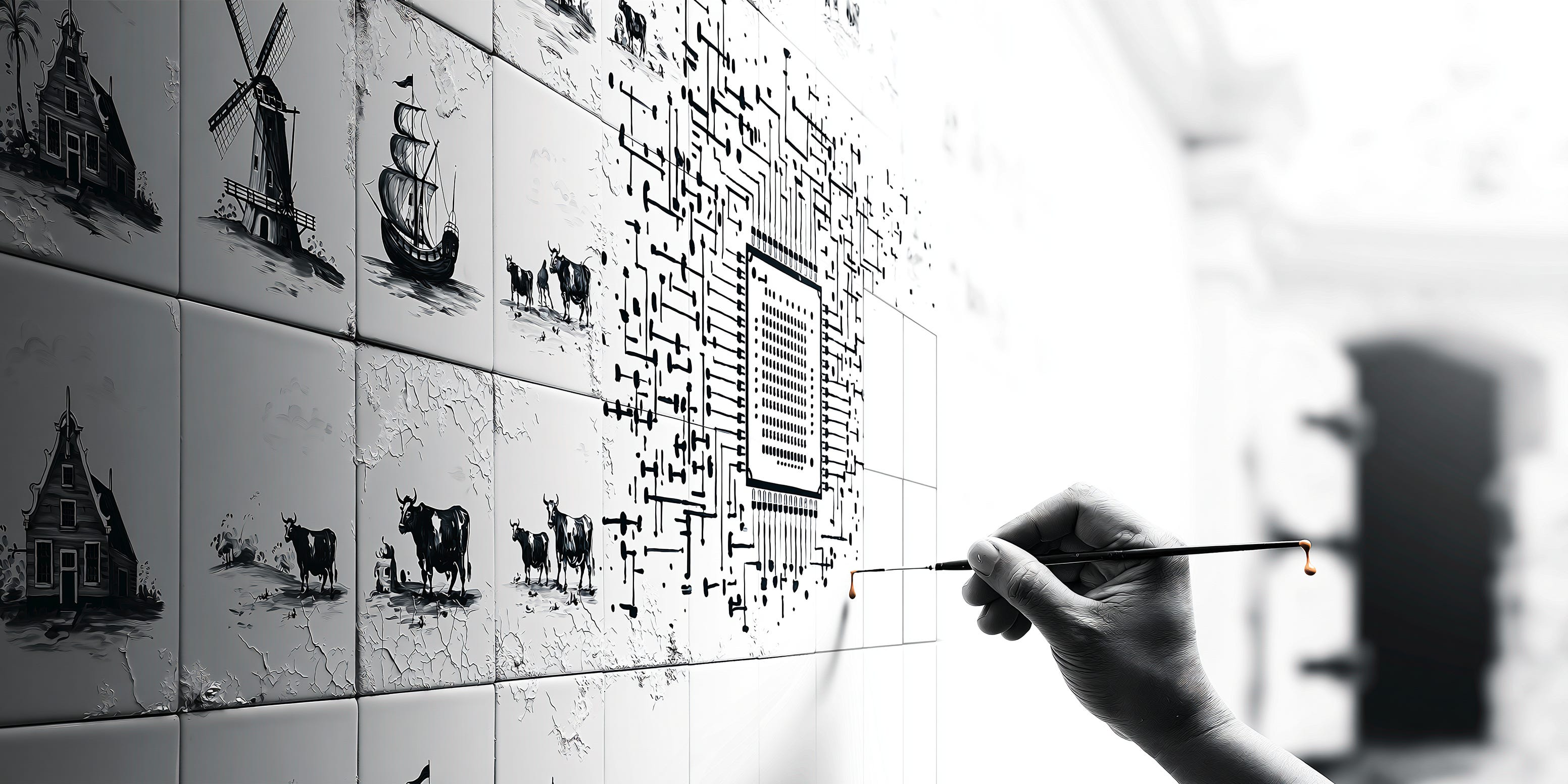
I recently visited Amsterdam on a work trip for a couple of days.
After a client meeting, we were sitting outside with a couple of local colleagues, having lunch in front of one of the main canals while enjoying one of those scarce warm and sunny days.
I looked around. Most people were doing the same, although the pace seemed less rushed. More relaxed. Others were swimming in the canal or just chatting shirtless beside it. Certainly, by the looks, everyone there seemed well-off.
Earlier that morning, I noticed pretty much the same while having a coffee walking to the office. Amsterdammers were moving but, to my eyes, there wasn’t much stress, speed or nervousness around. Also, again, they seemed to be in a fairly high economic stratum.
Honestly, I naively judged that by their clothing, watches, kind-of-polished looks and their vehicles.
On that latter front, although one sees mostly bikes, I also learned that morning that there is an unusually high concentration of premium and high-tech cars.
That made a question pop into my head.
Why are the Dutch rich? Where does the wealth of this rather small country come from?
The answer came straight from those colleagues: Trade (the port of Rotterdam is the largest and busiest in Europe) and specialization in high-value industries (agriculture, horticulture, specialty chemicals or food processing). Also, gas fields.
If you can get past the simplification, it is directionally correct.
“Ah. And that company that makes machines that make the chips,” said one of them.
She was talking about ASML.
Surely, in the fascinating process of generating intelligence out of sand, not many would expect the outskirts of Eindhoven to be one of the hotspots (if not the one).
ASML
ASML manufactures the most complicated machines ever created by humans. And not many of them.
It makes cutting-edge lithography machines. Basically, a printing press for microchips. These are fundamental for companies like TSMC, Samsung or Intel, who rely on them to fabricate the processors that range from CPUs and smartphone chips to, most notably, GPUs for AI training and inference.
Its market value sits at roughly $671 billion. Comfortably, the most valuable company in Europe and one of the top 20 worldwide.
That market cap equals about half of the entire Dutch economy’s annual output.
Revenues for this year are projected at north of €45 billion. And with around 44,000 employees, it runs margins that are exceptional for a hardware company: 52.8% gross margin for 2025.
ASML’s (so far) insurmountable moat is that it is the sole maker of tools that use extreme ultraviolet light (EUV). A type of light that does not naturally occur on Earth’s surface.
This allows ASML machines to consistently imprint chips at 5 nanometers (billionths of a meter) and below. The current state of the art sits at 2nm. And they are the only ones capable of doing so.
The “nanometer” figure historically referred to the size of the smallest feature you could print on the chip — roughly, how small each transistor was. But that number is no longer a literal physical measurement. Somewhere in the mid-1990s, “nanometers” stopped being a real dimension and became essentially a marketing label for a technology generation. So the 2nm chip is the successor to the 3nm.
In any case, smaller here is better in three dimensions:
More power — more transistors = more computing capability on one chip.
Speed — electrons travel shorter distances, so the chip can switch faster.
Efficiency — smaller transistors generally use less energy per operation, which means less heat and better battery life.
It projects to ship around 65 of these systems in 2026. Its most advanced systems are priced at around $380 million each, and all of them are strictly tracked and subject to export controls.
Miracle machines
ASML’s most advanced system is a 150-tonne machine, the size of two shipping containers.
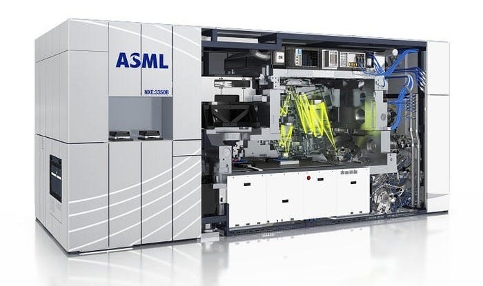
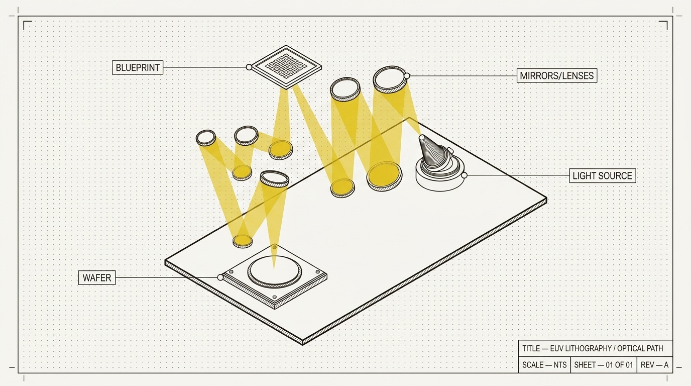
These lithography tools work on the same basic principle as an old slide projector: shine light through a patterned stencil — the “mask” — and project a shrunken image of a chip’s circuitry (the blueprint) onto a silicon wafer coated in light-sensitive chemicals.
Do this layer by layer, dozens of times, and you gradually build up a processor that can hold more than 100 billion transistors on a sliver of silicon about one and a half times the size of a postage stamp.
The catch is that the smallest detail you can print is set mainly by the wavelength of your light: shorter wavelengths act like a finer paintbrush.
For years the industry used deep-ultraviolet light, but to keep shrinking, ASML spent two decades commercializing something far harder — extreme ultraviolet light, or EUV, at a wavelength of just 13.5 nanometers, roughly one-fourteenth of what came before.
Generating that light is the part that looks like science fiction.
Inside the machine, droplets of molten tin about 25% the width of a human hair are fired into a vacuum at around 250 kilometers per hour and struck twice by a powerful laser.
A first pulse flattens each droplet into a pancake, and a second vaporizes it into a plasma several hundred thousand degrees hot, which flashes out a pinprick of EUV light.
This happens roughly 50,000 times a second. Because EUV is absorbed by air and even by ordinary glass, the whole process must run in a vacuum, and the light cannot be focused with lenses at all; instead it bounces off a series of mirrors made by Zeiss that are the smoothest objects ever manufactured — polished so precisely that, scaled up to the size of Germany, their largest bump would stand about a millimeter high.
Even so, each mirror absorbs some of the beam, and only a few percent of the light ever reaches the wafer.
Its newest “High-NA” systems squeeze features down to about 2 nanometers by using larger mirrors that gather light from a wider angle, while everything moves at ferocious speed and nanometer precision, the wafer stage accelerating harder than a fighter jet.
Transport is challenging. They get disassembled and transported by plane. It requires three Boeing 747 freighters, 40 shipping containers and 20 trucks for a single machine to be moved. Installation also requires ASML experts on site to set them up.
What it means
Although the race is on to replicate ASML technology, it will be extremely hard to get even close.
No other company makes machines that can reliably print chips at 7 nanometers and below. Even for more mature technologies, the firm’s tools account for over 90% of the market.
EUV occurs naturally in the Sun’s corona but not on Earth. It is also swallowed by air, glass and most materials (the things you’d normally build optics from), so the entire process is enclosed in a vacuum, steered by mirrors.
Also, the machine is an assembly of other people’s inventions. ASML counts 5,150 suppliers, and the top 35 of them carry 80% of its sourcing spend.
The mirrors belong to Zeiss, a German optics firm founded in 1846. The drive laser belongs to TRUMPF, also German. The light source subsystem belongs to Cymer in San Diego (which ASML eventually bought).
Besides mastering EUV light creation, a credible rival would need to rebuild that concentration of know-how and an equivalent supply chain.
The current production of these machines sits at around 65 EUV systems for 2026. ASML plans to add another 30% for 2027 and is investigating another 30% for 2028.
Demand by TSMC and others, at the current and projected pace, will probably outpace supply.
ASML — the sole maker of EUV lithography machines — becomes the ultimate physical ceiling on how much AI compute the world can build. Not chips, not money, but the machines that pattern the chips.
These are fascinating pieces of tech, bordering on science fiction. They may also be what prevents the world from getting broader synthetic superintelligence faster.
If you want expert help in making your AI strategy real for payments and finance, or need to build usable, production-grade agents, get in touch. That is part of the work we do for our clients in the AI Labs at Visa Consulting.